

Overview
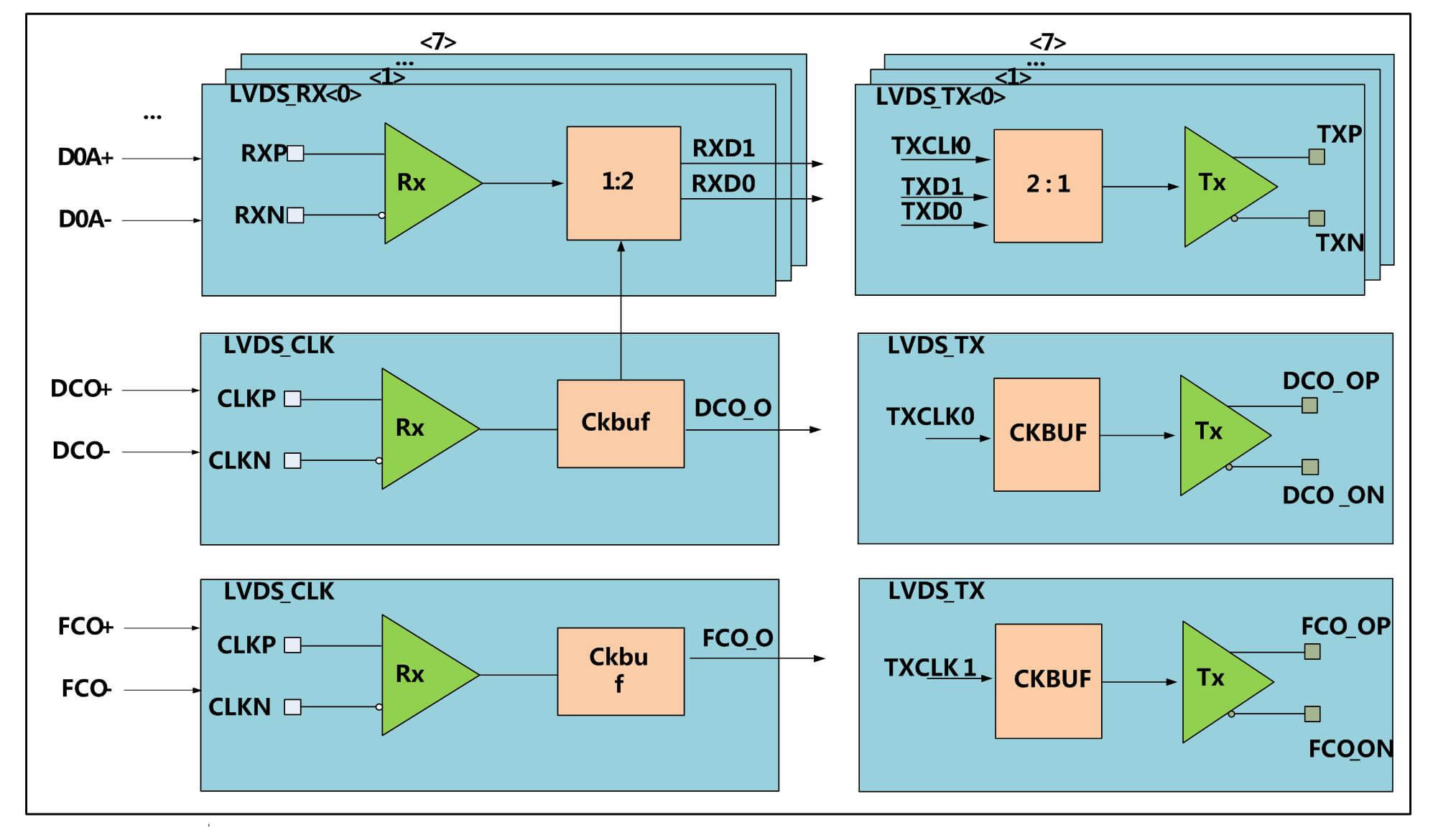
This IP is a high-speed LVDS (Low-Voltage Differential Signaling) transceiver supporting multi-channel joint. The LVDS TX & RX IP is specified for operation over the industrial temperature range. This IP operates from 3.3V/1.1V supply and works with 992Mbps data rate. It’s compatible with ANSI/TIA/EIA-644-A (LVDS) Standard.
Highlights
- • Compatible with ANSI/TIA/EIA 644-1995 LVDS standard
- • Multi-channel LVDS transceiver function
- • Maximum data transfer rate: 992Mbps (496MHz)
- • Typical output voltage: 350mV (100-Ω load)
- • Compatible with TTL level standard
- • Low power consumption
- • Operating junction temperature -40 ~125°C
- • Comprehensive consideration of area, power consumption and performance to achieve the optimal design
- • Support Flip Chip & Wire bond BGA package
Deliverables
- - GDSII&CDL Netlist
- - Verilog Model
- - LEF Layout Abstract(.LEF)
- - Liberty Timing Models(.lib)
- - Verify Results
- - Specification
- - Datasheet
- - Integration Guideline
- - Evaluation Plan
- - Leading support for package design, SI&PI modeling and production test development
Highlights
- • Compatible with ANSI/TIA/EIA 644-1995 LVDS standard
- • Multi-channel LVDS transceiver function
- • Maximum data transfer rate: 992Mbps (496MHz)
- • Typical output voltage: 350mV (100-Ω load)
- • Compatible with TTL level standard
- • Low power consumption
- • Operating junction temperature -40 ~125°C
- • Comprehensive consideration of area, power consumption and performance to achieve the optimal design
- • Support Flip Chip & Wire bond BGA package
Applications
-
Display System
-
Communication System